HARTING connectors in wafer scanners
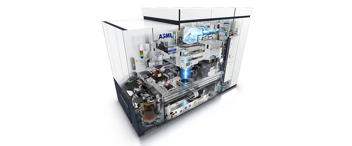
Wafer scanners are highly complex systems that are used to apply structures to semiconductor wafers. Without machines of this kind, today's information society would be unthinkable, since ICs, the core components of computers, cell phones, etc., could not be produced in large numbers.
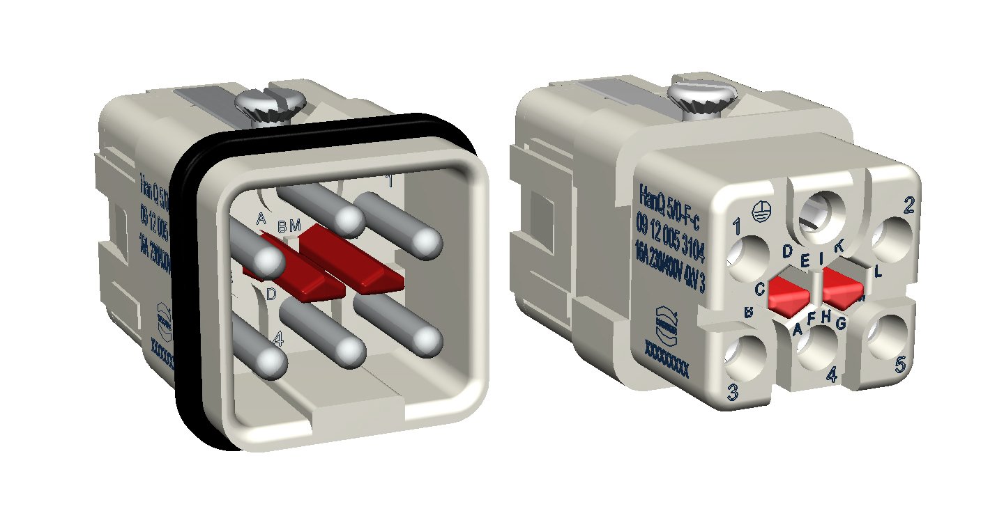
Wafer scanners and their components must be reliably powered. In order to use as little space as possible, compact connectors such as the Han® Q5 / 0 are used. This connector fits exactly into a housing of size Han® 3A and offers a total of 5 Han® E contacts (rated current: 16A, 230 / 400V) and a PE space.
In the case of partial assembly, a current of more than 35A can even be transmitted at an ambient temperature of 20 ° C. In combination with EMC housings, a very good shielding attenuation is also achieved - which ensures that the power transmission via the Han® Q5 / 0 does not disturb the surrounding electronics.
In addition, the variant for PCB adapter offers the option of soldering the Han® Q5 / 0 directly onto a printed circuit board. With this approach, users save themselves the otherwise complex wiring of the industrial connector to a terminal block on the PCB - which is not only costly, but also prone to error.


